


Next: Optional: analog division
Up: Advanced op-amp designs
Previous: Logarithmic amplifier
Analog multiplier
Combining log amps with adding amps allows one to build analog multipliers and
other components of analog computers (for a review, see Faissler, Ch. 30).
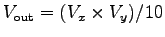
Here we examine the transfer functions of one such commercial device, AD534.
![$\textstyle \parbox{2.0in}{\raisebox{-1.25in}{\par
\hbox{\hskip 0in \vbox to 1.25in{\includegraphics[height=1.25in]{FIGS/fig4.8.ps}\vfill}}}}$](img106.png)
- For multiplication, use the fixed
 V supply from the job board as the
  input and use
several fixed voltages from the reference job board as the
input and use
several fixed voltages from the reference job board as the  input (V,
 V,
V,  V,
V,  V). Connect the
  input to the output. Connect the
  ,
,
 , and
, and  inputs to common. Test the multiplier in all four quadrants by
applying voltages of both polarities in the range of
inputs to common. Test the multiplier in all four quadrants by
applying voltages of both polarities in the range of  V. The
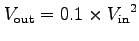
multiplier transfer function should be
V. The
multiplier transfer function should be
 .
Include in your
data set
.
Include in your
data set  values of
  ,
,  , and
, and  .
.
- Offsets modify the multiplier equation:
where  ,
,  , and
, and
 are the
  ,
,  , and output
offsets, respectively. Use your data to evaluate each of the offsets. Explain
how magnitude of offset-induced errors changes with and input levels.
, and output
offsets, respectively. Use your data to evaluate each of the offsets. Explain
how magnitude of offset-induced errors changes with and input levels.
- To obtain an output voltage proportional to the square of an input voltage,
connect both and inputs to the same voltage source and the and
inputs to common. The input remains connected to the output. Test
the circuit over a V range of voltages and compare to the expected
 .
.
- The ``squared voltage''output can be plotted against the input with the
 -mode of the oscilloscope. Substitute the output of the FG set in the
sine wave mode as the
source in the squaring circuit wired above. Connect the multiplier output to
the vertical scope input and the FG output to the horizontal. Use a
-mode of the oscilloscope. Substitute the output of the FG set in the
sine wave mode as the
source in the squaring circuit wired above. Connect the multiplier output to
the vertical scope input and the FG output to the horizontal. Use a  Hz
sine wave signal. Sketch the resulting display.
Hz
sine wave signal. Sketch the resulting display.
- Now use the dual-trace mode to observe the waveforms of the input and output
signals. Sketch a representative display and indicate the position of OV
for each waveform.
- Explain the relationship of the frequencies and the DC components of the input
and output waveforms.
Subsections
Next: Optional: analog division
Up: Advanced op-amp designs
Previous: Logarithmic amplifier
For info, write to: physics@brocku.ca
Last revised: 2007-01-05